| Search Engine | Site Map | FTP Site | Technical Support |
| Home | Data Sheets | Products | Press Room | Company Info | Sales Offices | ||||
| |||||||||
| Tech Brief No. 1 1-Wire Net Design Guide Dan Awtrey, Staff Engineer, Automatic Information Group | ||
| NOTE: In addition to the normal updates and
corrections, this tech brief now includes information on the Phantom
Presence pulse and expanded data on the DS2409. It also includes the
schematic for the DS9097U COM port adapter.
The 1-Wire Net, sometimes known as a MicroLAN is a low-cost network based on a PC or microcontroller communicating digitally over twisted-pair cable with 1-Wire components. The network is defined with an open drain (wired-AND) master/slave multidrop architecture that uses a resistor pull-up to a nominal 5V supply at the master. A 1-Wire Net based system consists of three main elements: a bus master with controlling software, the wiring and associated connectors and 1-Wire devices. Any standard microcontroller such as an 8051 with at least a 1.8MHz clock, as well as a PC using a 115.2 kbps-capable UART, can serve as master for the Net. The UART supplies 1-Wire timing by sending a byte for each 1-Wire bit, creating within the byte short and long time slots to encode the binary 1's and 0's. At this 14.4 kbps data rate (115.2 divided by 8 = 14.4 kbps) the PC can address a node on the bus and start receiving data in less than 7 milliseconds. Since timing is controlled by the UART, microprocessor clock speed does not affect the search time. Software such as TMEXTM to control and monitor bus activity is available for downloading at http://www.ibutton.com/software/tmex/index.html. | ||
|
1-Wire Net protocol uses conventional CMOS/TTL logic levels, where 0.8V or less indicates a logic zero and 2.2V or greater represents a logic one. Operation is specified over a supply voltage range of 2.8 to 6 volts. Both the master and slaves are configured as transceivers allowing data to flow in either direction, but only in one direction at a time. Technically speaking, data transfers are half-duplex and bit-sequential over a single pair of wires, data and return, from which the slaves "steal" power by use of an internal diode and capacitor. Data is read and written least significant bit first. An economical DS9097 COM Port Adapter is available to interface RS-232 to the Net. Newer more versatile adapters based on the DS2480 Serial 1-Wire Line Driver chip provide more capability such as active pull-up and slew-rate control. The DS2480 is designed to interface between RS-232 and the 1-Wire bus, generating the proper signals and programmable waveforms that provide maximum performance. Regardless of whether a DS9097- or a DS2480-based adapter is used, readily available, low-capacitance, unshielded, Category 5 twisted pair phone wire is recommended for the bus. As previously mentioned, data on the 1-Wire Net is transferred with respect to time slots. For example, to write a logic one to a 1-Wire device, the master pulls the bus low and holds it for 15 microseconds or less. To write a logic zero, the master pulls the bus low and holds it for at least 60 microseconds to provide timing margin for worst case conditions. A system clock is not required, as each 1-Wire part is self clocked by its own internal oscillator that is synchronized to the falling edge of the master. Power for operation is derived from the bus data line by including a half-wave rectifier onboard each slave. In Figure 1, whenever the data line is pulled high by the bus pull-up resistor the diode in the half-wave rectifier turns on and charges the internal 800pF capacitor. When it drops below the voltage on the capacitor, the diode is reverse-biased, isolating the charge. The isolated charge stored on the capacitor provides the energy source to power the slave during the intervals the bus is pulled low. The amount of charge lost during these periods is proportional to the time the bus is low. It is replenished when the data line again turns on the half-wave rectifier diode. This concept of "stealing" power from the data line by a half-wave rectifier is referred to as "parasite power." 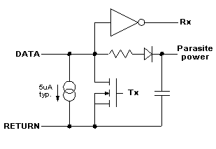 Figure 1: 1-Wire parasite power circuit.In operation, the master resets the network by holding the bus low for at least 480 microseconds, releasing it, and then looking for a responding Presence pulse from a slave connected to the line. If a Presence pulse is detected, it then accesses the slave by calling its address. The master issues any device specific commands required, and performs any needed data transfers between it and the slave. It controls the information transfer by generating time slots and examining the response from the slave. For a more detailed description of the communication sequence, refer to "So that's how it works!" in the Appendix. Complete technical and timing details are available in the Book of DS19xx iButton Standards. (Click Here for a copy.) The address of each device is stored in a lasered ROM section with its own guaranteed unique, 48-bit serial number that acts as its node address. With 248 serial numbers available, there will never be a problem with conflicting or duplicate node addresses on the LAN. This 48-bit serial number is just part of a 64-bit code programmed into each 1-Wire device at the factory. An 8-bit family code is stored in the first byte that identifies device type. The next 6 bytes store the unique individual serial number while the last byte contains a cyclic redundancy check sum (CRC) with a value based on the data contained in the first seven bytes. This allows the master to determine if an address was read without error. Floppy in a Button 1-Wire devices can be formatted with a file directory just like a floppy disk. This allows files to be randomly accessed and changed without disturbing other records. Information is read or written when a device connected to the bus is addressed by the master, or an identification badge or Decoder Ring is touched to a port somewhere along the 1-Wire Net. A typical access port consists of outer ring and insulated spring-loaded center conductors mounted in an appropriate housing. The ring touches the case of the iButton or Decoder Ring and connects it to the return line of the bus while the spring-loaded center contact connects the lid to the bus data line. The inclusion of memory in 1-Wire chips allows standard information such as employee name, ID number etc., to be stored within the device, with up to 64K available. For example, it would only take about one-fourth of the available memory to store the equivalent of a business card and digitized black and white ID photograph. This still leaves generous space for additional important data such as medical records, credit information or security level to be included. With such information literally "at hand" in the case of the Decoder Ring, reliable identification and access is readily available and machine readable. Memory devices are also useful for storing "tag" information for nodes on the bus and for sensor calibration or function information. Packaged and ready to go Because the 1-Wire Net only requires one wire plus return, iButtons can be packaged in a coin style battery case 16mm in diameter and 5.8mm thick. This is about the size of a stack of three dimes. The two-piece stainless steel package acts as both protective housing and electrical connection point. The case serves as return contact (ground) and the lid as data contact. The package size allows inclusion of a Lithium cell to provide 10 years of standby power to maintain data in volatile RAM memory when not connected to the LAN. A variety of memory configurations are available, including iButtons containing up to 64K of memory. 1-Wire devices that do not require a memory backup battery are also available in more traditional solder-mount packages.
SECTION 2: Working the LAN Control the slew rate of the driver In a typical system using a PC running Dallas' 1-Wire Operating System Software (TMEX) and using a COM port adapter, communication occurs in time slots of 8.68 microseconds under control of the UART. A communication cycle begins when the transistor in the master actively pulls the line to a logic zero. This one to zero transition is the synchronizing edge for all 1-Wire communications. A 1-Wire slave holds the zero if appropriate, and the resistor returns the line to the supply voltage after both the master and slave release the line. In ROM search, which is required to identify the devices on the bus, the most critical part of 1-Wire communication is the read data time slot, especially if a logic one is being transmitted. In the general case, there may be many arbitrarily placed devices on the bus, each seeing the falling edge of the time slot issued by the master at a slightly different time. Because communication requires that a signal travel the length of the cable and return, the electrical length of the bus must be less than one-half the time interval allowed for a single data bit slot. That is, round trip propagation time for a signal must be less than 4.34 microseconds (8.68 microseconds divided by 2). Devices beyond this range will not be seen by the master. In the COM port adapter, there is an active pull-down transistor that is either turned fully on or completely off under control of the PC or microprocessor. The falling edge generated by turning it on signals the start of a time slot on the Net. When the switch is turned off, the line is pulled toward the supply voltage by the bus pull-up resistor. Due to the rapid response and low impedance of the active pull-down transistor used to generate a logic zero, the signal fall time will be in the sub-microsecond range. If switching occurs in less time than the transition takes to traverse the electrical length of the cable and return, the 1-Wire Net is operating in a transmission line environment and reflections from the line end can cause disrupt communications. Normally, the solution would be to terminate the ends of the cable in its characteristic impedance with fixed resistors. These resistors would then absorb the energy that otherwise would be reflected by the impedance mismatch and cause problems. However, the recommended cabling has a 100 Ohm typical impedance which would result in the inability to generate a logic one with an acceptable pull-up resistor. It is interesting to note that since the port transistor inside 1-Wire slaves has a 100 Ohm on-resistance, the bus is properly terminated anytime one at the cable end is turned on. It may be possible on some 1-Wire Nets to AC terminate the bus using a series resistor and capacitor connected to ground. After the capacitor charges, it blocks DC current so the series resistor presents no load to the bus. During transitions however, the capacitor appears as a short circuit and the resistor terminates the line. A general rule of thumb for selecting the capacitor, is 3 times the rise time divided by cable impedance. For a 4 microsecond rise time on 100 Ohm cable, this works out to be 0.1µF. The disadvantage of AC termination is the bit dependent timing jitter it generates due to the charging and discharging of the terminating capacitor shifting the waveforms. Consequently, because it is not possible to terminate the end of the cable in its characteristic impedance with a fixed resistor, the slew rate of the bus master pull-down transistor must be controlled. For bus lengths of 100 meters or more a 1.1 volt per microsecond slew rate is recommended. This provides a one to zero transition that takes about 4 microseconds to ramp to the 0.8V logic low threshold. Because port transistors in 1-Wire devices only hold the line down after the bus master pulls it low, they do not normally exhibit slew rate problems. The exception is when a Presence pulse is generated in response to a Reset command from the bus master since the slew rate of the Presence pulse of a 1-Wire slave is essentially uncontrolled. Disruptive edge rates also occur when a new 1-Wire device is connected to the Net. Phantom Presence pulse If the Net consists of a fixed collection of 1-Wire slaves, the slew rate problem of their Presence pulse can be overcome by generating a "Phantom Presence Pulse" with the bus master. This is simply an artificial slew rate controlled Presence pulse created by the bus master that starts at 10µS and terminates at 60µS. A sample pulse can then be generated at 70µS to see if a slave is on the bus or node if desired. This technique masks the high slew rate of the slaves high-to-low Presence pulse transition because the bus is already at logic zero when they occur. However, the Phantom Presence pulse technique is obviously ineffective with new slaves which arrive at unpredictable times on the bus. 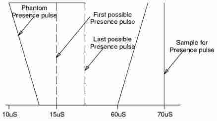 Figure 2: A Phantom Presence pulse can be started by the bus master prior to any possible Presence pulse from a slave. It must last long enough that the slowest possible Presence pulse will have started.Controlling the edge Figure 3 shows a suggested slew rate control circuit. The 2N7000 shown, is a commonly available general purpose n-channel FET, but transistor characteristics are not critical and almost any general purpose n-type transistor may be substituted. A bipolar type such as the 2N2222 may also be used with minor component value changes to provide the recommended slew rate. Refer to the Appendix for additional information and a 1-Wire waveform template. 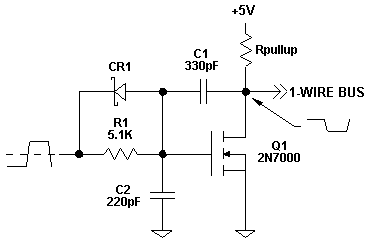 Figure 3: A controlled slew rate pull down for the 1-Wire net bus master. Transistor type is not critical.Pulling up the line Once both master and slave turn off, the bus pull-up resistor pulls the data line high. As the capacitive load on the Net increases by adding 1-Wire devices, the time to raise the data line to the supply voltage also increases. This also occurs when the network is lengthened due to the 50pF of capacitance added per meter of twisted-pair cable. This can be seen in Figure 4 as the number of slaves is increased from 1 to 300. If the product of the total capacitive load (including cable, device, stray capacitance, etc.), and the pull-up resistor value results in a time constant (RC) that exceeds the bit time slot defined by 1-Wire protocol, communication stops. Because grounding unused wires or shields in a cable adds capacitance which can significantly increase the RC time constant, they should be left disconnected. 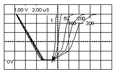
Figure 4: Loading effect of increasing the number of 1-Wire devices using active pull-up and 2m cable.As can be seen in Figure 6, the input capacitance of 1-Wire devices contribute to the capacitive load on the network. However, the 800pF parasitic power supply capacitance only exists at voltage levels above 2.8V minimum. Ignoring the capacitance of the parasitic power capacitor, the bus pull-up resistor value, together with the cable capacitance and 1-Wire device input capacitance represent the network time constant t. This is a reasonable omission since parasite capacitance does not become a factor until the bus has already passed the 2.2V logic one threshold. The network time constant determines the rate at which the data line returns to a logic one voltage. With the requirement that at t equals 13.02 microseconds (the data sample time) the 1-Wire voltage needs to have reached the 2.2V threshold of a logic one, the value of t can be calculated as follows: t = 13.02 µs / ln (Vs/(Vs-2.2V))=
22.4µs
Where Vs is the pull-up supply voltage. Using the recommended 1.5K minimum pull-up resistor value and 5V supply voltage, t is calculated as 22.4 microseconds. Assuming the Net is loaded with the maximum fanout as calculated in a later section, the cable capacitance alone must not exceed 12nF to yield a network time constant no more than calculated. Using 50 pF/m as typical cable capacitance implies that the theoretical maximum cable length is 240 meters. If the data sample time is recalculated with the new value of 21.7 microseconds, t becomes 37.4µs. This permits 22nF of cable capacitance, which represents a cable length that exceeds the maximum allowed round trip propagation time. The effect of cable capacitance can be seen in Figure 5, where 100 1-Wire devices were addressed at the end of a 2 or 100 meter cable. The 100 meter cable added 5000pF of capacitance. 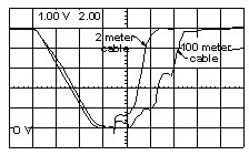 Figure 5: Effect of cable capacitance on signal driving 100 1-Wire devices. The 100m cable adds 5nF.The risetime can be improved by reducing the value of the pull-up resistor, using lower capacitance cable, shortening the cable, or reducing the number of devices on the bus. The pull-up resistor, however, should not be reduced below 1.5K Ohm. Reducing the value of the pull up resistor increases the logic zero voltage on the network, reducing system noise immunity. If the value of the pull-up resistor is already minimum, an active pull-up may be substituted. This also allows use of longer cables by decreasing the network time constant. Of course, the same rules apply to an active pull-up as to a pull down, and slew rate must be controlled when operating in a transmission line environment. The effect of residual current flowing in the bus when the active pull-up turns off can be seen in Figure 8. This was of little concern with a passive pull-up as an RC time constant has an inherently slow slew rate. One convenient source of an active pull-up is the MAX6314. This part was designed by MAXIM as a bidirectional open-drain µP reset for the 68HC11. However, it contains circuitry to automatically enable a 20mA p-FET pull-up for 2 microseconds when the data line exceeds a trip voltage of about 0.6V on the rising edge. Unfortunately, it does generate a logic zero output whenever the supply voltage drops below its reset threshold (its intended use). For use on the MicroLAN this can be detrimental as heavily loaded data lines can cause a reset, disabling communication, so selection of a part with a low reset threshold is suggested. One possibility is the MAX6314US31D3-T. This part has a 3-volt trip level that allows the supply to drop 2 volts before it generates a reset. The MAX6314 comes in a four-pin SOT143 package that requires little PCB area. Although the MAX6314 contains an internal 4.7K pull-up resistor, it is recommended that an external 2.2K resistor be added in parallel. This provides the equivalent of the recommended minimum 1.5K pull-up resistor, which results in the bus crossing the trip voltage in minimum time. The bus waveform then exhibits three distinct segments. When both the master and the 1-Wire devices release the data line, it starts rising at a rate determined by the value of the pull-up and the total capacitive load (RC time constant). When it passes its trip threshold of approximately 0.6V, the 20mA p-FET is turned on and accelerates the bus toward the supply voltage. If the bus is heavily loaded, the 2 microsecond one-shot may timeout with the bus well below the supply voltage. If this occurs, the 1.5K equivalent pull-up resistor continues to raise the bus voltage at the rate seen when the bus was first released. All three of these segments can be seen in Figure 4. This data however, was taken with a discrete proprietary design and not with the MAX6314. Refer to Appendix A for additional information on active pull-ups. The maximum voltage to which the bus pull-up resistor can raise the data line is determined by the product of the pull-up resistor value and the idle current of all devices on the line. The more devices, the greater the voltage drop across the pull-up resistor. The fanout limit of a particular 1-Wire Net is reached as the voltage drop across the pull-up resistor reduces the Net supply voltage to 2.8V. This is the minimum voltage that will recharge the parasitic power supply of the 1-Wire devices. From this, the maximum theoretical fanout may be calculated. It is equal to the supply voltage (Vs) minus 2.8V (the minimum operating voltage) divided by the pull-up resistor value. The resultant is divided by 15µA, the worst case device supply current. For a 5V supply and 1.5K minimum pull-up resistor value we have the following:
Fanout MAX = (5-2.8)/1.5K=1.47mA/15µA=98
devices
This represents the theoretical maximum number of 1-Wire devices that can successfully communicate with the master using a 1.5K pull-up resistor and 5V supply over worst case conditions of current and temperature. The assumptions being that all devices are drawing the maximum supply current and operating in a -40°C to 85°C environment. In the real world, all devices will only be drawing the 15µA maximum supply current during System Reset and Presence Detect. At that time all device oscillators turn on for 5T times. Since 1T time typically lasts 30 microseconds, 5T times represents 150 microseconds, with a worse possible case of 255 microseconds. Circuit design ensures that all 1-Wire devices will be able to operate from their internal parasite power source for the duration of this interval once fully charged. Thereafter, they will be drawing 5µA maximum which permits tripling the previously calculated fanout of 98. In addition, most systems will be operating over a much narrower temperature range which allows still larger fanouts. For example, in a typical lab environment, over 500 1-Wire devices in continuous communication had only a 1.2V drop across the pull-up resistor. This implies that typical idle current per device is less than 2µA when environmental and supply ranges are limited.
SECTION 3: It's all in the cable Take care in selecting a cable As previously mentioned, the 1-Wire Net consists of three segments: a bus master, the wiring and connectors and the 1-Wire devices as shown in the electrical equivalent circuit of Figure 6. The wiring between the master and the 1-Wire devices is modeled by the inductance and resistance of the data and return lines and the lumped capacitance of the cable. Cable capacitance is simply the product of cable length times unit capacitance. This is typically 50pF/m for the recommended Category 5 twisted-pair cable. Similarly, line resistance represents cable length multiplied by the specified resistance per meter of a single wire. A 1-Wire device is modeled by its input capacitance (Cin), a constant discharge current (Idisc), the parasitic power supply circuitry (Di, Ri, Cload) and its operating current (Iop) of 10 µA during communication. The 5µA idle current per 1-Wire device is required to keep its interface synchronized with the communication protocol. When the 1-Wire port transistor is on, its impedance is nominally less than 100 Ohm, which provides a 0.4V logic zero with a 4mA current sink. If multiple 1-Wire devices are residing on the bus, Cin, Idisc, Iop and Cload should be multiplied by the number of devices to determine the total. Ri needs to be divided by the number of devices. The port transistor inside the 1-Wire device allows it to place a logic zero on the network. Except for the presence detect cycle, Search, Skip and Read ROM commands, only one of them will be conducting when addressed by the bus master. 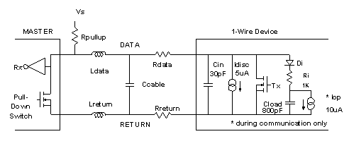 Figure 6: Electrical equivalent circuit of the 1-Wire Net.While parasitic resistance reduces the zero logic level noise margin of the digital signals, cable capacitance together with the parasitic power supply of 1-Wire devices adversely affect the size of the network. At power up, this capacitive loading requires several milliseconds to charge before communication can start on the Net, especially if a passive (resistive) pull-up is used. Also on long lines with many 1-Wire devices grouped at the end, the parasitic power requirements create a dip or slope change in the rising edge of the waveform at about 2.8V as the energy reservoirs of the devices are filled. Once filled, the recovery time after each time slot will be sufficient to maintain the charge. Figure 7 shows the effect charging the parasite power capacitance has on different numbers of 1-Wire devices at the end of 100 meters of Category 5 cable. Notice that the slope of the rising edge decreases as it crosses the 2.8V threshold finally reversing direction to form a dip when loaded with 100 or more devices. These "dips" become more pronounced the longer the bus remains low. Clearly the physical properties of the cable connecting the master and 1-Wire slaves strongly dominates the network. Comparison of the waveforms of Figure 4 taken with two meters of Category 5 cable to those of Figure 7 taken with 100 meters makes this plain. For short runs up to 30 meters, cable selection for use on the 1-Wire Net is less critical as the impedance characteristics are generally insufficient to have a marked, adverse effect on the bus. Even flat modular phone cable works with limited numbers of 1-Wire devices. However, the longer the 1-Wire Net, the more pronounced cable effects become, and therefore the greater importance placed on cable selection. 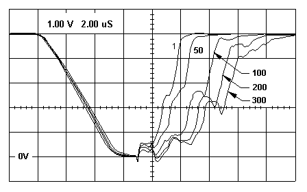 Figure 7: Parasite power loading of 0 to 1 transition. Notice that the dip becomes more pronounced with increasing number of devices at end of 100m cable.Given sufficient length, any cable exhibits transmission line effects. Real cables display distinct properties of resistance, capacitance and inductance, which in turn are determined by cable geometry, the size and spacing of the conductors and their surrounding dielectric. These physical properties define the characteristic impedance, the signal bandwidth supported and the propagation velocity of the cable. Specifically, cable resistance reduces the zero logic level noise margin, although values to 100 Ohms for the total cable length are acceptable. Cable capacitance however, which can range from 30pF/m to 100pF/m, loads the MicroLAN driver, increasing not only the network time constant (t) computed earlier, but also the peak current flowing in the cable as the master transistor turns on and discharges the line. If this transistor turns off before the charge stored in the line capacitance is completely discharged, the residual current left flowing in the line determines the amplitude of a transient voltage spike generated as a product of this current and the cable inductance. The resulting voltage spike seen at the driver can become large enough to interfere with communication. The effect of residual current flowing in the cable when the bus pull-down transistor and the active pull-up turns off can be seen in Figure 8. Notice that in each case, the spike generated is in the direction of the opposite rail. 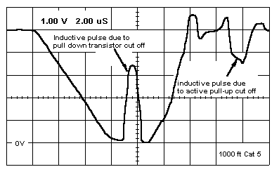 Figure 8: Inductive generated voltage spikes such as seen here, may occur on long lines due to residual current flow when pull down or pull-up circuits turn off.At the far end of the cable, when the pull down transistor turns off its inductively generated voltage spike swings negative, reverse biasing the substrate of the 1-Wire device closest to the cable end which clamps the voltage excursion at a diode drop. This device then will not respond to the master. The problem is the differential inductance, which is that measured across the cable input when the two wires of the line are shorted together at the far end. Differential inductance is substantially lower than the inductance of a single wire because the current flows in opposite directions in the pair and in the ideal case would cancel completely. Because differential inductance decreases as the distance between conductors is reduced, use of adjacent and preferably, twisted pair is recommended. Twisted pairs help reduce unwanted coupling from nearby interference sources because the currents induced in the wires flow in opposite directions in the two conductors and tend to cancel. Another concern is that the recommended category 5 unshielded twisted pair phone cable is available with two or more pairs. While the capacitance between wires in a pair is approximately 50 pF/m; that between wires of different pairs is closer to 30 pF/m. Because grounding the unused wires will add this 30 pF/m to the 1-Wire capacitive load, shields and unused wires need to be left unconnected at both ends of the cable. Grounding them can increase the capacitive load to the point that the bus pull-up cannot raise the line above the logic switching threshold within the bit time slot and communication stops. Refer back to Section 2 and the discussion of network time constant in "Pulling up the line" for more information. It is also not recommended to simultaneously run two 1-Wire Nets in the same cable bundle, because the capacitive load varies dynamically dependent upon data pattern, which can lead to erratic operation. Keep the bus running As line inductance increases, the product of L di/dt can generate voltage excursions that cause bit errors and reverse bias the substrate of at least the first 1-Wire device at the far end of the cable. These voltages spikes are generated by the current still flowing in the data and return lines of the cable when the transistor in the master is turned off before the charge stored in the line capacitance is fully discharged. The obvious and recommended solution is to maintain the pull-down transistor in the on state until the current in the line discharges. If it is not possible to stretch the timing, a Schottky diode placed across the bus at the far end is suggested to clamp the inductive generated voltage overshoot. Connect the diode across the cable with the cathode on the data line, and the anode on the return. Only one diode is required for each branch.
SECTION 4: Rewiring the LAN The DS2409 MicroLAN Coupler If the network is heavily loaded, and/or very long, it may be preferable or even necessary to separate the bus into sections. This has the added benefit of providing information about the physical position of a 1-Wire device on the bus. By using one section as the main "trunk," and adding or removing segment "branches" to it with a DS2409 as needed, a true MicroLAN is created. It is also possible of course to add or remove additional segments to the branches using a MicroLAN Coupler as the node control. This approach reduces the capacitive and idle current loads the bus master sees to that of the trunk and those segments connected to it by activated DS2409s. However, the limitations to the total capacitive load, idle current and line length covered in earlier portions of this document still apply. That is, for the trunk and activated sections of the LAN, the capacitive load must be low enough to allow the bus pull-up to raise the line above the logic one threshold within the time slot. The combined idle current of the 1-Wire devices must not reduce the supply voltage below 2.8V. And the electrical length of activated cable must allow a transition from the master to reach the cable end and return within the time slot. The DS2409 MicroLAN Coupler is a key component for creating complex MicroLANs. It contains the MAIN and AUX transmission gate outputs, plus an open drain CONT output transistor, each of which can be remotely controlled by the bus master over the 1-Wire network. Both the MAIN and AUX outputs support a "smart-on" command which generates a reset/presence sequence on the selected output before connecting to the 1-Wire bus. This allows a subsequent ROM function command to apply only to the devices on the just activated segment. The DS2409 requires a 5V supply without which it shorts the 1-Wire bus and no communication is possible. Since the DS2409 contains no user-available memory, the AUX output can be used to label the node by connecting a 1-Wire memory chip to store the required data. Tagging protocol information is available on the Dallas Semiconductor Automatic Information Software Development FTP site. A simple MicroLAN BRANCH with EEPROM labels connected as described is shown in Figure 9. 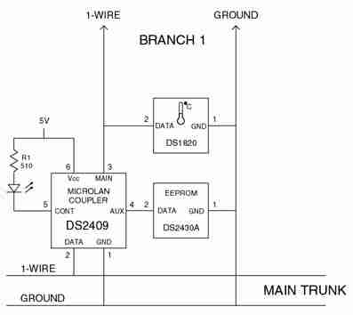 Figure 9: Separating the 1-Wire bus into branches using the DS2409 MicroLAN Coupler.In the example, a DS2430 EEPROM is connected to the DS2409 AUX output. This provides tagging information specific to that particular node such as location, function, etc. The LED attached to the CONT output provides visual indication of the specific branch being addressed and can be caused to flash via software for extra visual impact. A single DS1820 Digital Thermometer is shown on the branch output but multiple 1-Wire devices can be placed as required. To avoid loading the entire 1-Wire Net with the capacitance associated with routing power along with the 1-Wire DATA and GND, the CONT output of the DS2409 can be used to operate a pass gate transistor to switch the 5V supply along with the MAIN output switching the branch. The MICREL MIC94031 transistor shown in Figure 10 contains the gate pull-up resistor shown, so implementing the circuit requires only the addition of single SOT-23 package. By default, whenever the MAIN output of the DS2409 is turned on, the CONT output is pulled low, turning on the pass gate and routing power to the selected branch. Turning MAIN off automatically turns CONT and therefore the pass gate off, so no software revisions are required for the circuit. The DS2409 is available in a 6-pin TSOC surface-mount package. For further information about the DS2409, please refer to the datasheet. 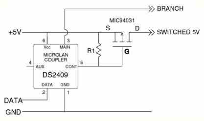 Figure 10: Method of switching local power to a branch using a DS2409 and a pass transistor.The DS2406 is a low-side addressable switch intended for remote control, perhaps in combination with an opto-coupler or relay, or to provide visual indication of an operation or end-of-limb by means of an LED (Light Emitting Diode). The DS2406 is not recommended as a means for providing branches on the MicroLAN, because branching requires use of a high side switch. This is because current flowing through the on-resistance of the port transistor develops a voltage that raises the ground pin of all devices connected to it above the ground reference. Since the 1-Wire devices will be hard wired to the data line, whenever the bus master outputs a logic zero the potential on the data pin becomes negative with respect to the voltage on its ground pin. This polarity acts to forward bias various p-n junctions in the 1-Wire devices resulting in device dependent disruptions. For example, when this voltage reaches approximately minus 0.3V, it can continuously activate the POR (power-on-reset) of any attached DS2406, effectively removing it from the bus. The DS2406 addressable switch was designed to perform closed-loop control of its two open drain output transistors, PIO-A and PIO-B, over twisted pair cable up to 300 meters from a PC. Each output can also sense and report to the PC the logic level at its port. When turned on by the bus master, the PIO-A port is connected to the IC ground pin and can sink up to 50mA, and hold off a maximum of 13V, while the PIO-B sinks 8 mA and holds off 6.5V. The on-resistance of the DS2406 PIO-A output transistor is about 10 Ohms, whereas the PIO-B output is about 50 Ohms. The off impedance of both addressable switches exceeds 10 Meg Ohms. The DS2406 is available in a 6-pin TSOC surface-mount package, or a single channel (PIO-A) version in a TO-92 package. For more information on the DS2406 dual addressable switch which contains 1K of one time user programmable EPROM, please refer to the datasheet.
SECTION 5: Policing the LAN Protection and Noise All 1-Wire Net compatible devices contain built-in ESD (electrostatic discharge) protection circuitry able to withstand ± 10kV minimum Human Body Model ESD events. However, when interfacing a computer to a 1-Wire Net it is good engineering practice to provide additional means to protect the system from ESD and EMI (electromagnetic interference) damage. Economical protection can be provided at the bus master by means of diodes shorting negative spikes or feeding positive ones higher than 5V to the power supply where they are absorbed by capacitors and other protection devices. When selecting protection diodes or surge suppressors, choose devices with minimum junction capacitance and fast switching times. Two good examples are the ERA82 Schottky diode from FUJI or the more common 1N5817. The BAT54x series of Schottky diodes available in the SOT-23 surface mount package is also acceptable. If 1-Wire EPROM parts will not be programmed using the RS-232 to 1-Wire interface adapter, excellent protection can be provided with a single DS9502 ESD protection diode. These behave like a 7.5V zener diode during normal operation. However, if the voltage across them exceeds their 9V trigger voltage they fold back to 5.5V. If exposed to an ESD hit beyond their ratings, the DS9502 will eventually fail shorted, preventing damage to the protected circuitry. The DS9502 is available in a 6-lead TSOC package, or as solder-mount "bumped" die. Introducing the DS2480 In order to reduce the engineering load of setting up a 1-Wire Net, Dallas Semiconductor has developed the DS2480 Serial 1-Wire Driver. This IC connects directly to UARTs and 5V RS-232 systems. Adapters are available using the DS2480 that connect directly to a standard COM port and provide 1-Wire outputs. The IC contains programmable pull-down slew-rate control and an active pull-up. Other features include support for data rates of 9.6 (default), 19.2, 57.6 and 115.2 Kbps and programmable 1-Wire timing. The DS2480 is available as the DS9097U, which is a DB9 to RJ11 COM port adapter and the DS1416D with DB9 to dual blue dot receptors. These are true ground adapters, Crypto-capable with FCC Class B approval. It's the results that count By applying information presented in this tech brief such as using Category 5 twisted pair, controlling slew rates and substituting an active pull-up, reliable communication over 300m of cable with more than 500 assorted 1-Wire devices was demonstrated. Without slew rate control and active pull-up, the limit is about 100 meters with 150 1-Wire devices. Recommendation summary for operating long or heavily loaded MicroLANs
APPENDIX A: Hardware for the 1-Wire Net PC to 1-Wire Net adapters Any PC with a UART capable of 115.2 kbps can serve as bus master for reading and writing 1-Wire devices on the Net. However, a serial COM port to 1-Wire adapter is needed to interface the computer RS-232 levels to the 5V 1-Wire bus. A schematic for the DS9097 COM port adapter developed by Dallas Semiconductor as an economic and easy to use interface, is shown in Figure 11. The adapter is powered entirely from the computer COM port. Note that the circuitry makes maximum use of the UART controlled output using only clamping and level shifting diodes. Although this provides a simple and reliable circuit that directly couples to the serial port, it lacks a ground reference. While not of concern in operating the Net, it can present complications during trouble shooting, as the oscilloscope ground cannot be connected to the 1-Wire return. Connecting the DS9097 1-Wire return to ground can result in permanent damage to the adapter. 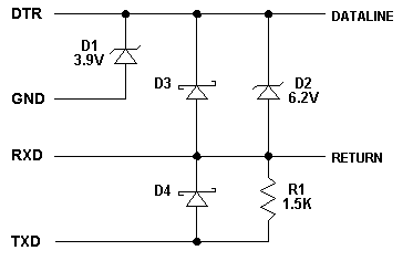 Figure 11: The DS9097 COM port adapter. Note that "return" is not ground. R1 is the bus pull-up.In Figure 11, current limiting and slew rate control are provided by the UART as RS-232 requirements, while zener D1 clamps the data line at 3.9V. Zener diode D2 limits the maximum voltage range on the 1-Wire bus to 6.2V. It also restricts the most negative voltage swing on RXD to minus 2.3V. When TXD is positive, Schottky diode D3 limits the voltage difference between the 1-Wire data and return lines to 0.2V, and D4 connects TXD to RXD. This bypasses R1 the passive bus pull-up, and provides a low impedance path to initiate a time slot. The 1.5K minimum value pull-up resistor generates a 0.3V logic zero across the 100 Ohm on-resistance of a 1-Wire device. Since the maximum voltage still recognized as a logic zero is 0.8V, this leaves 0.5V of noise margin. The DS9097 comes with a DB9 for attachment to a PC serial port and an RJ-11 for connecting to the 1-Wire Net. The same circuit is available in a DB9 to DS9098 socket as the DS1413. A DS9097E version in a DB25 case is also available for programming EPROM based 1-Wire products such as the DS198x series. It provides a power jack to accept an external 12V auxiliary supply as required. A true ground COM port adapter If the return line of the Net must be grounded at some point, a true ground COM port adapter interface is required. The schematic for a true ground adapter is given in Figure 12. Its positive supply is derived from DTR and RTS by Schottky diodes CR1 and CR2, and filter capacitor C1. A well-regulated 5 volts is provided by the low dropout LP2980 voltage regulator as long as the COM port provides at least 5.1V. If the positive level of DTR and RTS drops below this the regulator drops out of regulation. CR3 and C3 provide the negative supply required by the DS275 RS-232 Transceiver Chip from TXD during read data and idle time slots. The DS275 connects directly to the 1-Wire Net and converts it's CMOS/TTL levels to the RS-232 levels required by the UART. If surface mount components are used, the circuitry will fit comfortably on a 0.6" by 0.9" printed circuit board. This can be mounted inside a DB9 female to RJ-11 PC adapter. A slew rate controlled pull down Because it is not possible to terminate the ends of the cable in its characteristic impedance, the slew rate of the bus transistor must be controlled to prevent adverse transmission line effects. For more information on this subject, refer back to Section 2 and "Control the slew rate of the driver." In Figure 12, transistor Q1 and the components associated with its gate, limit the slew rate to about 1.1 volts per microsecond. This provides a one to zero transition that takes about 4 microseconds to ramp from the 10 to 90% points. This has proven to be adequate for cable lengths exceeding 300 meters. The 2N7000 shown is a commonly available general purpose n-channel FET, but transistor characteristics are not critical and almost any general purpose n-type transistor may be substituted. A bipolar type such as the 2N2222 may also be used with a base resistor and minor component value changes to provide the recommended slew rate. In the pull-down circuit of Figure 12, Miller integrator capacitor C5 across Q1 acts as the primary slew rate control element. On lightly loaded LANs using about 50 devices on 50 meters or less of cable, it may be possible to eliminate C5. Sufficient slew rate control is then provided by R1 and C4. In operation, when TXD switches from its minus 12V rail to the plus 12V rail, the signal is passed to the gate of Q1 by input resistor R1. This transition is slowed and delayed slightly by the RC time constant of R1 and C4. When the voltage level at the gate reaches the threshold voltage of Q1, the transistor begins to turn on. The effect of the transistor turning on with C5 across its terminals results in a nearly linear voltage ramp from the supply voltage to ground. This one to zero transition on the bus is the synchronizing edge for 1-Wire communications. Q1 remains in the on state for the duration of time that TXD is held at plus 12V by the UART. Afterward, the bus is returned to the supply voltage by the action of pull-up resistor R2. Zener diode D1 serves several functions in the circuit. It protects the gate of Q1 by limiting positive voltage excursions to 12V, and negative ones to minus 0.6V. Gate input resistor R1 limits the current through the zener. The capacitance of D1 also adds to that of C4, helping control the transistor transition. While they are not shown for clarity, good engineering practice would place reverse-biased Schottky diodes across the output of the circuit. One diode should be from the supply voltage to the data line, the other from the data line to ground. Use of ultra-fast low-capacitance Schottky diodes such as the ERA82 from FUJI is suggested. The BAT54x series available in SOT-23 packages is also acceptable. 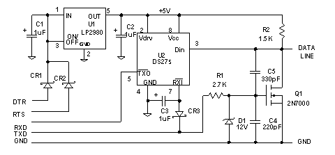 Figure 12: A PC serial COM port to 1-Wire Net true ground adapter. Q1 is the slew rate controlled pull-down and R2 is the passive bus pull-up resistor.A cycle in the sequence of 1-Wire Net communication over the true ground COM port adapter would proceed as follows. Initially, TXD would be at minus 12V (an RS-232 "mark" or logic one), so the gate of Q1 would be clamped at minus 0.6V by the reverse bias on zener diode D1. Consequently Q1 is off, and the bus will have been raised to the 5V supply by pull-up resistor R2. When TXD switches between the minus 12V and plus 12V rails, Q1 will be turned on and ramp the bus voltage down at the rate set by the Miller integrator capacitor C5. This one to zero transition has two paths, one continues down the bus, the other returns to the UART through U2. The signal returned to the UART, will be used to determine when to reexamine its registers for a response from a 1-Wire device on the bus. Meanwhile, the transition traveling down the bus is received sequentially by any attached 1-Wire slaves as the edge propagates past them. If this signal from the UART is a Reset pulse, it lasts for at least 480 microseconds and then releases the bus. The bus pull-up raises the line to the supply, and approximately 30 microseconds later the UART reexamines its registers to see if a Presence pulse is being sent by a 1-Wire device. In the interim, the internal oscillators and controllers within each 1-Wire device have determined that a Reset has been sent and at the appropriate time will pull the bus low. The exact time the bus is pulled low and its duration, is a function of individual device variation. The fastest will pull the bus low first, and the slowest release it last. When the final 1-Wire device releases, the pull-up resistor raises the bus toward the supply voltage at a rate determined by its value times the capacitive load it sees on the line (RC time constant). If the pull-up cannot raise the bus above the logic one threshold within the time slot, the master will always see a logic zero and conclude the line is shorted. Consequently, communication cannot occur. Assuming however that the timing is acceptable, the UART sees a proper Presence pulse indicating there are 1-Wire devices on the bus. It then proceeds to call serial numbers to identify them. In order to write logic one or zero values onto the bus, the UART turns on Q1 for short (less than 15 microseconds), or long (greater than 60 microseconds) time slots respectively. To read, the UART begins by turning on Q1 for a short time slot exactly as if a logic one was being sent. If this time slot remains unchanged, the UART defines this as reading a logic one. If a 1-Wire slave extends the time slot initiated by the master by continuing to hold the line low (even though the UART has released Q1 and R2 attempts to pull the data line high) the UART defines this as reading a logic zero. 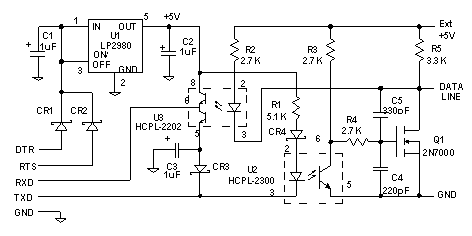 Figure 13: An optically isolated COM port to 1-Wire Net adapter.An optocoupler-isolated adapter In some applications, because of ground loops, or for safety reasons, it is necessary to provide galvanic isolation between the computer master and the Net. For such cases, the optically-coupled circuit in Figure 13 is suggested. Optical isolation of the COM port requires special purpose optocouplers, such as the high speed, low input current HCPL-2300 used in the transmit section. An HPCL-2202 with 20V totem pole output is used in the 1-Wire to RS-232 channel. The HCPL-2300 has an LED input that only uses 0.5mA, and an output transistor with 200 nanosecond maximum propagation time. In the circuit, the LED current is set with resistor R1, but a current source such as the J503 or CR056 from Siliconix will provide superior performance over the diversity of logic levels available with RS-232. If a constant current source is not used it may be necessary to recalculate the value of R1 to maintain 0.5mA with the plus and minus voltages in use on a particular RS-232 COM port. CR4 is required to protect the LED, as it only has a 5V breakdown in the reverse direction. In operation, the HCPL-2300 coupler U2, provides the necessary isolation and level shifting from the double rail plus and minus 12V RS-232 to the single rail 1-Wire Net. The coupler is connected in a non-inverting configuration, so when TXD is at minus 12V, the LED input is on. Consequently, the coupler output transistor is also on and the bus pull-down transistor Q1 is off. With Q1 off, bus pull-up resistor R5 holds the LAN at the supply voltage. U3, the receive optocoupler is also off, so its output is at minus 12V. When TXD changes state, the HCPL-2300 input LED is reversed-biased, turning the coupler output transistor off. Its collector is then pulled high by resistor R3. This zero to one signal is slowed and delayed slightly by the RC time constant of R4 and C4. When the voltage level at the gate reaches the threshold voltage of Q1, the transistor begins to turn on. The effect of the transistor turning on with Miller capacitor C5 across its terminals results in a nearly linear voltage ramp from the supply voltage to ground. When Q1 pulls the data line to ground, it also turns on the LED in U3 the HCPL-2202 coupler, causing its totem-pole output stage to switch to plus 5V. This transition will be received by the UART and used to determine when to reexamine its registers for a response from any 1-Wire devices on the bus. The data line remains at ground until TXD returns to its original state, and Q1 along with any 1-Wire slaves turn off. At that time, the bus pull-up resistors (R5 in parallel with R2) raise the data line toward the 5V supply at a rate determined by their equivalent value times the capacitive load seen on the line (RC time constant). This turns off the input LED of U3, and causes its output stage to switch to the minus RS-232 voltage level. Assuming the pull-up can raise the bus above 2.2V within the time slot, the UART will see a logic one, and communication proceeds. If the pull-up cannot raise the bus above the logic threshold within the time slot, the master will always see a logic zero and conclude the line is shorted. Consequently, communication stops. An active pull-up On a 1-Wire Net where the minimum acceptable pull-up resistor value
cannot raise the data line above the logic one threshold within the time
slot, an active pull-up must be used. Obviously, an active pull-up circuit
should be on only during a defined range of the rising edge (zero to one
transition). Conversely, it should not respond on the falling edge, nor be
active during logic zero time intervals. It must trigger on the rising
edge at about 0.9V plus or minus 0.1V to provide acceptable noise margin.
Preferably, once triggered it will remain on until the line is raised
above a specified threshold In Section 2 under "An active pull-up," use of the MAX6314 is suggested as an available circuit. This part was designed by MAXIM as a bidirectional reset intended for use with the 68HC11 microprocessor. As such, an important function of the chip is to monitor the supply voltage and assert a reset (logic zero) during power-up, power-down, or during supply droop. This obviously is an undesirable function on the Net. However, the part includes an active pull-up to solve the RC time constant problem faced on a high capacitance bus. Coincidentally, this consists of a p-FET in parallel with a 4.7K pull-up resistor (the maximum 1-Wire Net value). The FET is turned on for 2 microseconds when the waveform on the reset pin exceeds 0.9V maximum by a comparator triggered one-shot. Additional control circuitry ensures that the active pull-up is disabled at all other times. Operation of the MAX6314 when connected to the 1-Wire Net bus proceeds as follows. When the bus (connected to the MAX6314 reset pin) is pulled below 0.5V by the master, a comparator sets an internal flip-flop enabling the active pull-up control circuitry. When the bus is released, the internal 4.7K pull-up resistor starts raising the bus toward Vs (the bus supply voltage) at a rate determined by it's RC time constant. This generates a ramp that starts at the logic zero level and ends at the trip voltage of a comparator. When the trip voltage of the active pull-up enable comparator is exceeded, it triggers a 2 microsecond one-shot that turns the 20mA p-FET on. This starts a second much steeper ramp that begins at the comparator trip voltage and ends at Vs. However, if the bus is heavily loaded, a third ramp may be created if the 2 microsecond one-shot times out, and the bus voltage has not reached Vs. This ramp starts where the one-shot times out, and ends at the maximum voltage to which the passive pull-up can raise the line with the idle current load of 1-Wire devices on the bus. This third ramp will have a slope similar to the first. The characteristic waveform produced by an active pull-up is illustrated in Figure 14. 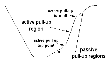 Figure 14: Characteristics of an active pull-up.Although the MAX6314 contains an internal 4.7K pull-up resistor, it is suggested that an external 2.2K resistor be added in parallel. This reduces the value to the equivalent of the recommended 1.5K minimum pull-up resistor, and allows the bus to cross the enable trip voltage of the active pull-up in minimum time. The combination of the MAX6314 and 2.2K resistor can be substituted for R2 in Figure 12 to provide a true ground COM port adapter with active pull-up. 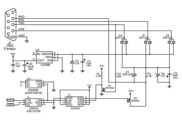 Figure 15: The schematic for the DS2480 based DS9097U COM port Adapter.In order to reduce the engineering load of setting up a 1-Wire Net, Dallas Semiconductor developed the DS2480 based series of COM port adapters. The basic schematic shown in Figure 15 is used throughout the series, the major difference being the type and number of 1-Wire connections on the output. The DS2480 provides programmable slew-rate control on the pull-down and an active pull-up. Other features include support for data rates of 9.6 (default), 19.2, 57.6 and 115.2 Kbps and programmable 1-Wire timing. The DS2480 also provides a strong pull-up mode to facilitate the higher current requirements of devices such as the DS1820 temperature sensor during conversion. The DS2502 shown is used to provide the adapter ID. The DS2480 is available with and without an ID in a DB9 to RJ11 COM port adapter as the DS9097U-009 and DS9097U-S09 respectively. The circuitry is also available as the DS1411 with a DB9 to DS9098 iButton socket and the DS1416D with DB9 to dual blue dot receptors. All adapters are true ground Crypto-capable adapters with FCC and CE approval.
APPENDIX B: Waveform template for a 1-Wire Net exceeding 100 meters
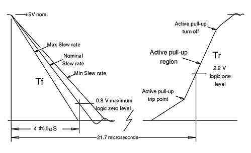 Figure 16: Waveform template for a 1-Wire Net exceeding 100 meters.This section defines the 1-Wire template for use with bus lengths extending 100 meters or longer. Notice that the zero to one transition is shown with the characteristic waveform for an active pull-up as the use of a passive pull-up resistor can be problematic with cables of this length. A 5V pull-up supply is recommended, but it can range from 3 to 6 volts. The falling edge(Tf) The one to zero (falling) transition of the bus master pull-down transistor is the system timing edge. It should have a 1.1volt per microsecond (V/µS) slew rate. As shown in the template, this requires 4 microseconds to cross the 0.8V logic zero threshold level. This slew rate provides acceptable performance with bus lengths up to 300 meters. It performs well over that range with 1-Wire loading varying from one to 500 devices. For Net communication to be successful, the bus must be raised to a voltage above the 2.2V logic one level before the master samples. Beginning with TMEX v3.0, sampling occurs 21.7µS after the master pulls the bus low. If the bus pull-up does not raise the voltage above the logic one threshold before sampling occurs, the master will always see a logic zero and conclude the bus is shorted. Consequently, communication can not occur. The rising edge(Tr) As the number of 1-Wire devices on the bus grows, the time required to raise the line above the logic one threshold increases. This also occurs as the network is lengthened due to the 50pF of capacitance added per meter of twisted-pair cable. Because of these effects, for a 1-Wire Net of 100 meters or more, an active pull-up must be used. Obviously, an active pull-up circuit should be on only during a defined range of the rising edge (zero to one transition). Conversely, it should not respond on the falling edge, nor be active during logic zero time intervals. It must trigger on the rising edge at about 0.9V plus or minus 0.1V to provide acceptable noise margin. Preferably, once triggered it will remain on until the line is raised above a specified threshold (3V or greater ) rather than for a set time interval (one-shot). This insures that the data line will be raised above the 2.8V level required to recharge the parasite power capacitors regardless of load. The maximum current the circuit can supply should be limited to about 15mA. Larger currents flowing in cable inductance can cause problems. Please consult the Dallas Semiconductor iButton website at http://www.ibutton.com/ for current product information, application notes and data sheets. |
| Updated
2000/10/25 Problems or comments? |
 Copyright © 2000 Dallas Semiconductor Corp. |